- 您现在的位置:买卖IC网 > Sheet目录308 > ADP5501ACPZ-RL (Analog Devices Inc)IC LED DRVR WHITE BCKLGT 24LFCSP
�� ��
��
��ADP5501�
�APPLICATIONS� INFORMATION�
�CONVERTER� TOPOLOGY�
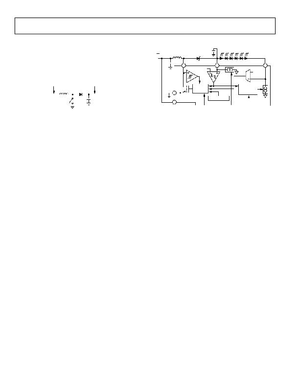
�VBAT�
�4.7μH�
�1μF�
�The� ADP5501� backlight� driver� uses� a� dc-to-dc� step-up� (boost)�
�converter� to� achieve� the� high� voltage� levels� required� to� drive� up�
�to� six� white� LEDs� in� series.� Figure� 43� shows� the� basic� asynchronous�
�boost� converter� topology.�
�1μF�
�2�
�SW�
�27V�
�I-LIMIT�
�22�
�BST�
�AUTO�
�LOAD�
�FB�
�BL_SNK�
�0.65V�
�23�
�VIN�
�VOUT�
�PGND�
�1�
�BOOST�
�CONTROL�
�OVP�
�BACKLIGHT�
�CURRENT�
�CONTROL�
�VBAT�
�21�
�THERMAL� S/D�
�Figure� 43.� Basic� Asynchronous� Boost� Converter� Topology�
�Assuming� an� initial� steady� state� condition� where� the� switch� has�
�been� open� for� a� long� time,� the� output� voltage� (VOUT)� is� equal� to�
�the� input� voltage� (VIN),� minus� a� diode� drop.�
�If� the� switch� is� closed,� the� output� voltage� maintains� its� value� as�
�the� diode� blocks� its� path� to� ground.� The� inductor,� however,� has�
�a� voltage� differential� across� its� terminals.� Current� in� an� inductor�
�cannot� change� instantaneously,� so� it� increases� linearly� at� a� rate� of�
�di� /� dt� =� VIN� /� L�
�where� L� is� the� inductance� value� in� henrys.�
�If� the� switch� is� kept� closed,� the� current� increases� until� the� inductor�
�reaches� its� saturation� limit,� at� which� point� the� inductor� becomes�
�a� dc� path� to� ground.� Therefore,� the� switch� should� be� kept� closed�
�only� long� enough� to� build� some� transient� energy� in� the� inductor�
�but� not� so� long� that� the� inductor� becomes� saturated.�
�When� the� switch� is� opened,� the� current� that� has� built� up� in� the�
�inductor� continues� to� flow� (because� the� current� in� an� inductor�
�cannot� change� instantaneously),� so� the� voltage� at� the� top� of� the�
�switch� increases� and� forward� biases� the� diode,� allowing� the�
�inductor� current� to� charge� the� capacitor� and,� therefore,� increase�
�the� overall� output� voltage� level.� If� the� switch� is� opened� and�
�closed� continuously,� the� output� voltage� continues� to� increase.�
�Figure� 44� shows� the� boost� configuration� used� in� the� ADP5501.�
�A� Schottky� diode� is� used� due� to� its� fast� turn-on� time� and� low�
�forward� voltage� drop.� An� input� capacitor� is� added� to� reduce� ripple�
�voltage� that� is� generated� on� the� input� supply� due� to� charging/�
�discharging� of� the� inductor.� An� integrated� power� switch� is� used�
�to� control� current� levels� in� the� inductor.� A� control� loop� consisting�
�of� a� feedback� signal,� some� safety� limiting� features,� and� a� switch�
�drive� signal� complete� the� boost� converter� topology.�
�Figure� 44.� Boost� Configuration�
�The� ADP5501� uses� a� current-limiting,� pulse� frequency� modu-�
�lation� (PFM)� control� scheme.� For� medium� to� large� output�
�currents,� the� converter� operates� in� pseudo� continuous� conduc-�
�tion� mode� (CCM).� It� generates� bursts� of� peak� current� limited�
�pulses� (600� mA� typical)� in� the� inductor,� as� shown� in� Figure� 9.�
�For� light� output� currents,� the� converter� operates� in� pseudo�
�discontinuous� conduction� mode� (DCM).� It� generates� bursts� of�
�small� (200� mA,� typical)� and� medium� (400� mA,� typical)� current�
�pulses� in� the� inductor,� as� shown� in� Figure� 11.�
�To� maintain� reasonable� burst� frequencies� during� very� light� load�
�conditions,� an� automatic� dummy� load� feature� is� available.� When�
�enabled,� the� 1� mA� dummy� load� is� activated� if� the� backlight� sink�
�current� code� drops� below� 8� while� in� linear� law� mode� or� if� the�
�backlight� sink� current� code� drops� below� 32� while� in� square� law�
�mode.�
�Safety� Features�
�The� ADP5501� uses� an� overvoltage� protection� (OVP)� circuit� that�
�monitors� the� boosted� voltage� on� the� output� capacitor.� If� the�
�LED� string� becomes� open� (due� to� a� broken� LED),� the� control�
�circuit� continually� commands� the� boost� voltage� to� increase.�
�If� the� boost� level� exceeds� the� maximum� process� rating� for� the�
�ADP5501,� damage� to� the� device� can� occur.� The� ADP5501� boost�
�converter� has� an� OVP� limit� of� 27� V� (typical).�
�The� ADP5501� also� has� a� feature� that� ramps� down� the� backlight�
�code� when� an� OVP� condition� is� detected.� This� may� be� useful� in�
�conditions� where� LEDs� with� marginally� high� forward� voltages�
�are� used� in� low� ambient� conditions.� The� feature� can� be� enabled�
�by� setting� the� OVP_EN� bit� in� Register� 0x02.�
�The� ADP5501� also� features� a� thermal� shutdown� circuit.� When�
�the� die� junction� temperature� reaches� 150°C� (typical),� the� boost�
�converter� shuts� down.� It� remains� shut� down� until� the� die�
�temperature� falls� by� 10°C� (typical).�
�Rev.� 0� |� Page� 26� of� 28�
�发布紧急采购,3分钟左右您将得到回复。
相关PDF资料
ADP8863ACPZ-R7
IC LED DRVR WHIT BCKLGT 20-WLCSP
ADUM1100UR
IC DIGITAL ISOL/COUPLER 8SOIC
ADUM1201CR
IC ISOLATOR DIGITAL DUAL 8SOIC
ADUM1210BRZ
IC ISOLATOR DIGITAL DUAL 8SOIC
ADUM1233BRWZ-RL
IC ISOLATR DGTL 2CH 0.1A 16-SOIC
ADUM1234BRWZ-RL
IC ISOLATR DGTL 2CH 0.1A 16-SOIC
ADUM1250SRZ-RL7
IC ISOLATOR 1MBPS 4CH 2.5K 8SOIC
ADUM1286CRZ
ISOLATOR DGTL 3KVRMS 2CH 8-SOIC
相关代理商/技术参数
ADP5501-EVALZ
制造商:Analog Devices 功能描述:SINGLE CHANNEL BOOST CONVERTER - Boxed Product (Development Kits)
ADP5520
制造商:AD 制造商全称:Analog Devices 功能描述:Backlight Driver with I/O Expander
ADP5520ACPZ-R7
功能描述:IC LED DRVR WHITE BCKLGT 24LFCSP RoHS:是 类别:集成电路 (IC) >> PMIC - LED 驱动器 系列:- 标准包装:6,000 系列:- 恒定电流:- 恒定电压:- 拓扑:开路漏极,PWM 输出数:4 内部驱动器:是 类型 - 主要:LED 闪烁器 类型 - 次要:- 频率:400kHz 电源电压:2.3 V ~ 5.5 V 输出电压:- 安装类型:表面贴装 封装/外壳:8-VFDFN 裸露焊盘 供应商设备封装:8-HVSON 包装:带卷 (TR) 工作温度:-40°C ~ 85°C 其它名称:935286881118PCA9553TK/02-TPCA9553TK/02-T-ND
ADP5520ACPZ-RL
功能描述:IC LED DRVR WHITE BCKLGT 24LFCSP RoHS:是 类别:集成电路 (IC) >> PMIC - LED 驱动器 系列:- 标准包装:6,000 系列:- 恒定电流:- 恒定电压:- 拓扑:开路漏极,PWM 输出数:4 内部驱动器:是 类型 - 主要:LED 闪烁器 类型 - 次要:- 频率:400kHz 电源电压:2.3 V ~ 5.5 V 输出电压:- 安装类型:表面贴装 封装/外壳:8-VFDFN 裸露焊盘 供应商设备封装:8-HVSON 包装:带卷 (TR) 工作温度:-40°C ~ 85°C 其它名称:935286881118PCA9553TK/02-TPCA9553TK/02-T-ND
ADP5520ACPZ-RL1
制造商:AD 制造商全称:Analog Devices 功能描述:Backlight Driver with I/O Expander
ADP5520-EVALZ
功能描述:EVAL BOARD FOR ADP5520 RoHS:是 类别:编程器,开发系统 >> 评估板 - LED 驱动器 系列:- 标准包装:1 系列:PowerWise® 电流 - 输出 / 通道:20mA 输出及类型:1,非隔离 输出电压:17V 特点:可调光 输入电压:2.7 ~ 5.5 V 已供物品:板 已用 IC / 零件:LM3508 相关产品:LM3508TLX-ND - IC LED DRVR WHT BCKLGT 9USMDLM3508TLDKR-ND - IC LED DRVR WHT BCKLGT 9MICROSMDLM3508TLCT-ND - IC LED DRVR WHT BCKLGT 9MICROSMDLM3508TLTR-ND - IC LED DRVR WHT BCKLGT 9MICROSMD
ADP5520XCPZ-R7
功能描述:IC LED DRIVER RGLTR DIM 24LFCSP 制造商:analog devices inc. 系列:* 零件状态:上次购买时间 标准包装:1
ADP5585
制造商:AD 制造商全称:Analog Devices 功能描述:Keypad Decoder and I/O Expansion GPIO functions GPIO functions